By Lisa Zyga from Phys.org:

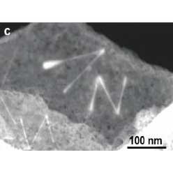
Images taken by a scanning transmission electron microscope (STEM) of electron ink on graphene paper, showing the letter “N” and the symbol “Ʌ.” Credit: Wei Zhang, et al. ©2013 IOP Publishing Ltd.
The researchers, Wei Zhang and Luise Theil Kuhn at the Technical University of Denmark in Roskilde, Denmark; and Qiang Zhang and Meng-Qiang Zhao at Tsinghua University in Beijing, China, have published their study on using electron ink to write on graphene paper in a recent issue of Nanotechnology.
“The ability to record information has been directly correlated with the process of human civilization since ancient times,” Wei Zhang told Phys.org. “Paper and ink are the two essential factors to record history. Currently, information communication has proceeded onto an unprecedented scale.”
Nanoscale writing, which is essentially the manipulation of matter on the nanoscale, has already been widely explored. The current methods can be classified into two groups: lithography (top down), which imprints a pre-made pattern on a substrate, but has restricted resolution; and self-assembly (bottom up), which manipulates atoms or molecules individually, but faces challenges with controllability.
Herein, the researchers proposed a combination method based on both types of methods to overcome the difficulties of each, which they demonstrated on “the thinnest paper in the world”: graphene.
“The rise of graphene calls for broad attention,” Qiang Zhang said. “One distinct characteristic is its flatness, which provides the perfect opportunity to be regarded as the thinnest paper. In order to directly write on this ultimate thin paper, the suitable ink must be found. At the small scale, typically nanoscale, the ink candidate must meet the qualification as both high-resolution writing and visualization function. Therefore, high-energy electrons in a transmission electron microscope (TEM) are the best choice. The electron beam can be manipulated as ink for direct writing, but is by itself invisible.”

When an electron beam (green) writes on graphene paper, some of the carbon atoms in the graphene are kicked off, and external carbon atoms are deposited onto the dangling bonds to form an irregular structure that appears as “ink.” Credit: Wei Zhang, et al. ©2013 IOP Publishing Ltd.